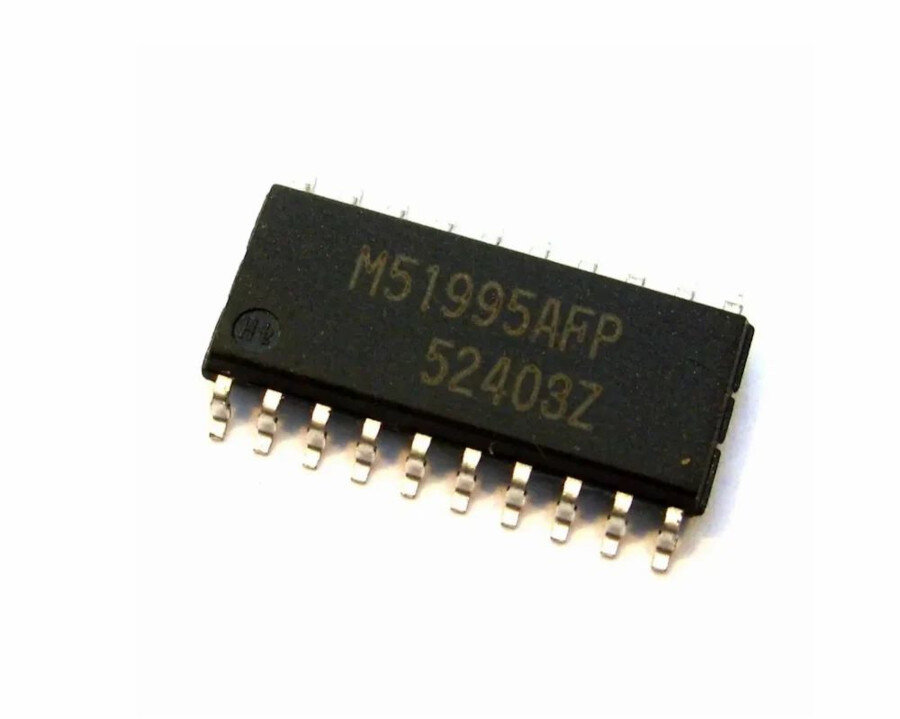
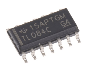
M51995AFP Switching Regulator Control SMD IC
Inhouse product
-
 ৳320.00
Reviews & Ratings
M51995A is the primary switching regulator controller which is especially designed to get the regulated DC voltage from AC power supply. This IC can directly drive the MOS-FET with fast rise and fast fall output pulse. Type M51995A has the functions of not only high frequency OSC and fast output drive but also current limit with fast response and high sensibility so the true "fast switching regulator" can be realized. It has another big feature of current protection to short and over current,owing to the integrated timer-type protection circuit,if few parts are added to the primary side. The M51995A is equivalent to the M51977 with externally resettable OVP(over voltage protection)circuit. COLLECTOR VOUT EMITTER VF ON/OFF OVP DET F/B
FEATURES
500kHz operation to MOS FETOutput current...............................................................±2AOutput rise time 60ns,fall time 40nsModified totempole output method with small through current Compact and light-weight power supplySmall start-up current............................................90µA typ.Big difference between "start-up voltage" and "stop voltage" makes the smoothing capacitor of the power input section small. Start-up threshold 16V,stop voltage 10VPackages with high power dissipation are used to with-stand the heat generated by the gate-drive current of MOS FET. 16-pin DIP,20-pin SOP 1.5W(at 25°C) Simplified peripheral circuit with protection circuit and built-in large-capacity totempole outputHigh-speed current limiting circuit using pulse-by-pulse method(Two system of CLM+pin,CLM-pin)Protection by intermittent operation of output over current...............................................................Timer protection circuitOver-voltage protection circuit with an externally re-settable latch(OVP)Protection circuit for output miss action at low supply voltage(UVLO) High-performance and highly functional power supplyTriangular wave oscillator for easy dead time setting HEAT SINK PIN
APPLICATION
Supply voltage to 36V Operating frequency.................................less than 500kHz Oscillator frequency setting resistanceT-ON pin resistance to 75kT-OFF pin resistance to 30k
VCC 7.1V 5.8V ON/OFF UNDER VOLTAGE LOCKOUT VOLTAGE REGULATOR 3K 500 F/B DET GND
OSCILLATOR RESISTANCE T-ON (ON duty) OSCILLATOR RESISTANCE T-OFF (OFF duty)
Symbol VCC VC IO VVF VON/OFF VCLMVCLM+ IOVP VDET IDET VFB ITON ITOFF Pd K Topr Tstg Tj Parameter Supply voltage Collector voltage Output current VF terminal voltage ON/OFF terminal voltage CLM-terminal voltage CLM+terminal voltage OVP terminal current DET terminal voltage DET terminal input current F/B terminal voltage T-ON terminal input current T-OFF terminal input current Power dissipation Thermal derating factor Operating temperature Storage temperature Junction temperature Peak Continuous Conditions Ratings Vcc +125 150 Unit mA W mW/°C °C
Note 1."+" sign shows the direction of current flow into the IC and sign shows the current flow from the IC. 2.This terminal has the constant voltage characteristic to 8V,when current is supplied from outside.The maximum allowable voltage is 6V when the constant voltage is applied to this terminal.And maximum allowable current into this terminal 5mA. 3.The low impedance voltage supply should not be applied to the OVP terminal.
SWITCHING REGULATOR CONTROL ELECTRICAL CHARACTERISTICS (VCC=18V, Ta=25°C, unless otherwise noted)
Operating supply voltage range VCC VCC(START) Operation start up voltage VCC(STOP) Operation stop voltage Vcc IccL IccO Icc OFF Icc CT Icc OVP VTHH ON/OFF VTHL ON/OFF VTHON/OFF IFBMIND IFBMAXD IFB VFB RFB VDET IINDET GAVDET VTHOVPH VTHOVP ITHOVP IINOVP VCCOVPC VCC(STOP) -VCCOVPC ITHOVPC fTIMER ITIMECH TIMEOFF/ON VTHCLMIINCLMTPDCLMVTHCLM+ IINCLM+ TPDCLM+ Difference voltage between operation start and stop Stand-by current Operating circuit current Circuit current in OFF state Circuit current in timer OFF state Circuit current in OVP state
ON/OFF terminal high threshold voltage ON/OFF terminal low threshold voltage ON/OFF terminal hysteresis voltage
15.2 9.0 Vcc=Vcc(START) -Vcc(STOP) Vcc=25V Vcc=9.5V F/B terminal input current F/B terminal input current IFB=IFBMIND-IFBMAXD F/B terminal input current=0.95mA VTHOVP=VTHOVPH-VTHOVPL VOVP=400mV OVP terminal is open. (high impedance) -5Ta85°C VCLM+=0V
Terminal voltage Terminal resistance Detection voltage Input current of detection amp Voltage gain of detection amp OVP terminal H threshold voltage OVP terminal hysteresis voltage OVP terminal threshold current OVP terminal input current OVP reset supply voltage Difference supply voltage between operation stop and OVP reset Current from OVP terminal for OVP reset Timer frequency Timer charge current OFF time/ON time ratio CLM- terminal threshold voltage CLM- terminal current Delay time from CLM- to VOUT CLM+ terminal threshold voltage CLM+ terminal current Delay time from CLM+ to VOUT
Frequently Bought Products
Product Queries (0)
Login Or Registerto submit your questions to seller
Other Questions
No none asked to seller yet
-
৳320.00